 FOLYSKY(WuHan) LTD.
 FOLYSKY(WuHan) LTD.


The detailed product introduction is as follows
1. Materials
① . 96% alumina ceramic ②. 99% aluminum nitride ceramic. Sapphire ④. High borosilicate glass
2. Conductor process
DPC (direct copper plating) 0.1-10oz LAM (laser copper plating) 0.1-10oz
3. Performance
Copper bonding force (N/cm2): ≥ 20 Thermal conductivity (W/m.K):
96% alumina ceramic 20-27 W/m K aluminum nitride ceramic 180-220 W/m K
Sapphire 27-30 W/m K high borosilicate glass 2-5W/m K
Warpage degree (mm): ≤ 2%
4. Substrate material
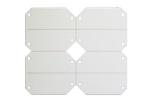
Commonly used large material size mm: 120 * 120 127 * 127 132 * 132140 * 130 190 * 140
Common large material thickness mm: 0.254 0.38 0.5 0.635 0.8 1.0 1.2 1.5 2.0
1.2, 1.52.0 need to be customized in advance, with a customization time of 20 days
5. Drilling
5.1 Minimum aperture: 0.075mm
5.2 Aperture taper tolerance:+/-10%;
5.3 Borehole offset:+/-0.02mm;
5.4 Slot hole tolerance:
Length ≥ 2 times width: long edge+/-0.05mm, wide edge+/-0.025mm; Length<2 times width: long side+/-0.025mm, wide side+/-0.010mm;
6. Electroplating on one side and two sides
Table Copper Thickness (Ounces)
H/H 1/1 2/2 3/3 4/45/5 6/6 7/7 8/89/9 10/10 can achieve perfect sealing of the conductive hole through electroplating, achieving no hole marks on the surface of the conductive hole. Surface roughness of electroplated copper: ≤ 0.3UM
7. Line
7.1 Line alignment tolerance: ± 0.045mm;
7.2 Minimum line width and line spacing: 0.1/0.1mm;
8. Resistance welding
8.1 The unspecified ink thickness shall be controlled as follows (if the customer specifies the ink thickness, it shall be controlled according to the customer's requirements) Line surface: ≥ 10um; ② Line angle: ≥ 8um; ③ Substrate: ≥ 15um;
8.2 Cofferdam ink thickness: 70-120 um;
8.3 Resistance welding alignment tolerance: ± 0.045mm;
8.4 Minimum width of solder mask wire:


Follow us

customer service